Visible to Intel only — GUID: kly1432262039272
Ixiasoft
1.1.2.2. Setting Up the Simulation Environment
- Follow the guidelines in Getting Started with the Design Store to download and install the reference design files.
- Open the reference design .qpf file after successfully installing the design templates.
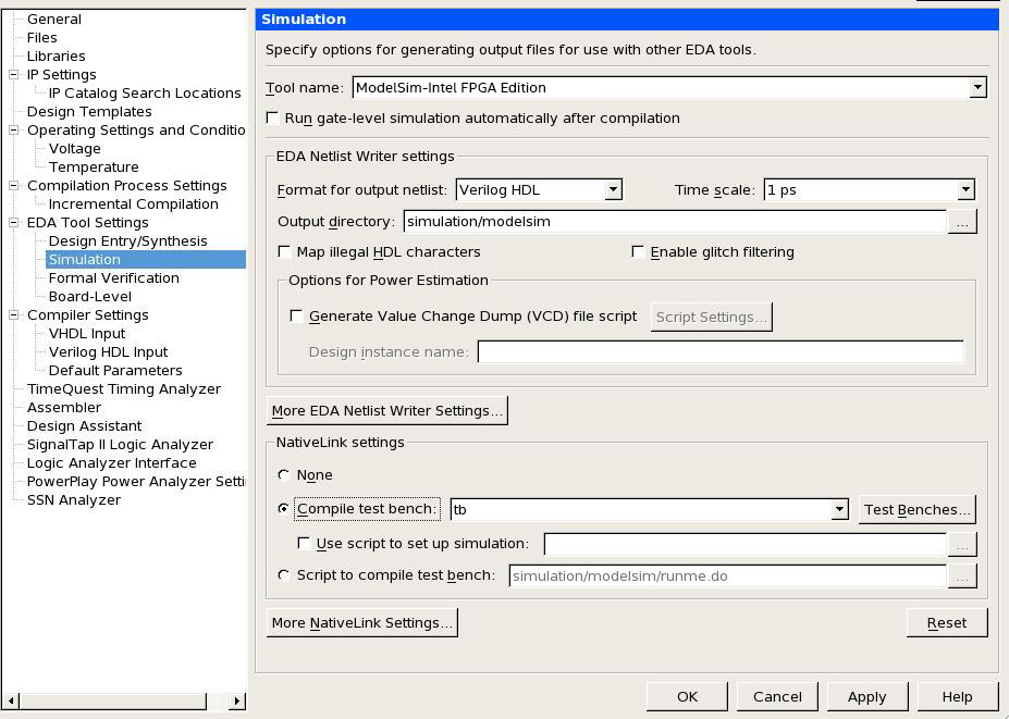
- Click on Assignments -> Settings....
- Select EDA Tools Settings -> Simulation.
- At the Settings window, choose ModelSim* - Intel® FPGA Edition for Tool Name. You may choose VHDL, Verilog HDL or System Verilog as the output netlist format.
Figure 2. Simulation Settings using EDA Tools in the Intel® Quartus® Prime Software
- Open dut_INPUT.qsys file and make sure the IP has the same configuration shown below:
Figure 3. Configuration for dut_INPUT Module
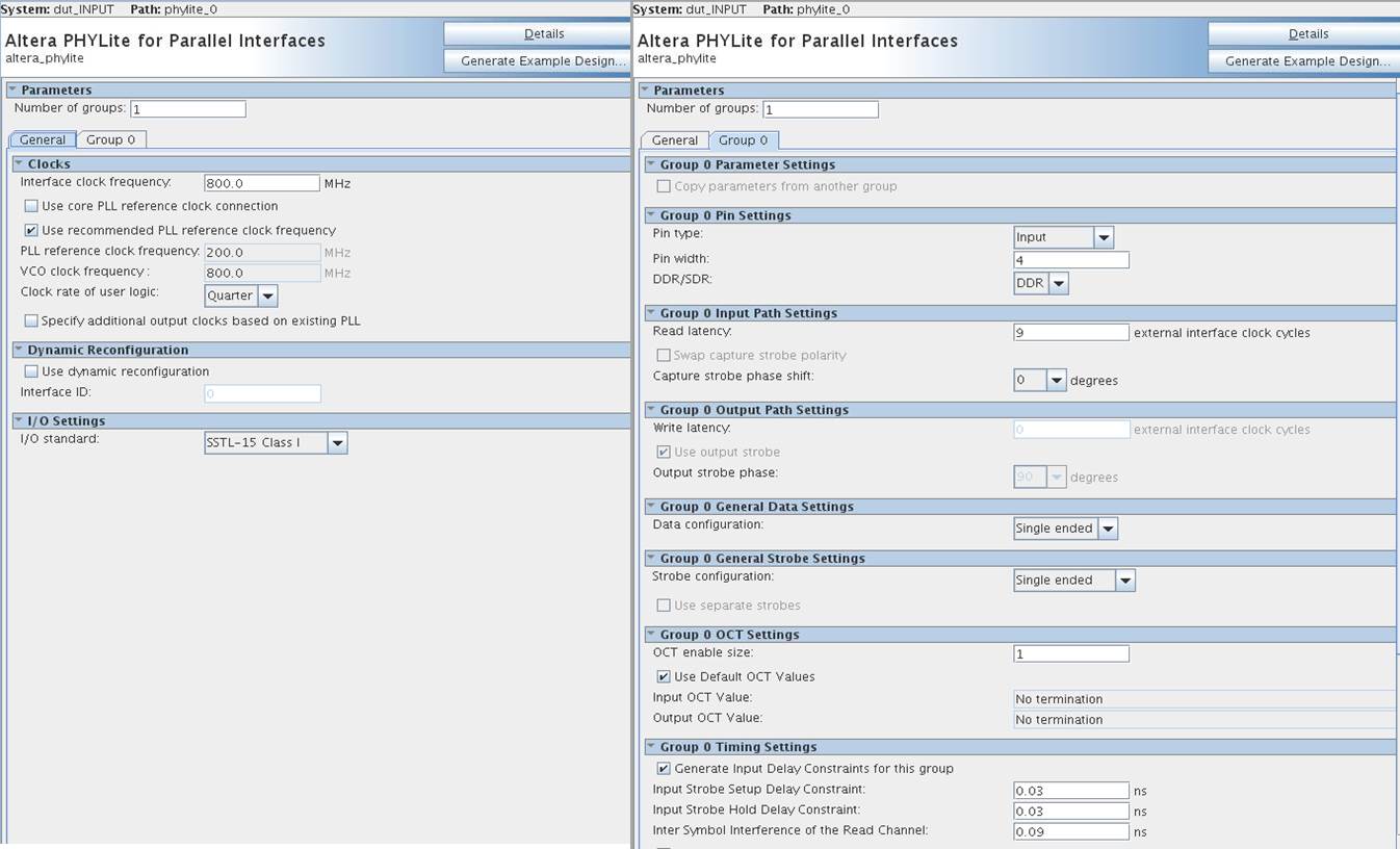
- Make sure that the Capture strobe phase shift is set to 0 degrees to align the incoming data to strobe edge during data transfer.
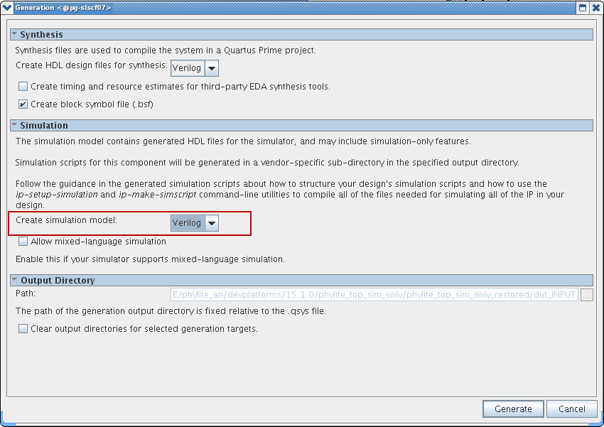
- Click Generate HDL... and select your desired simulation model format. Next, click Generate to generate the simulation model for the dut_INPUT module. Click Close and Finish when the generation is complete.
Figure 4. Generating Simulation Model
- From the Intel® Quartus® Prime software, open dut_OUTPUT.qsys file and make sure the IP has the same configuration shown below:
Figure 5. Configuration for dut_OUTPUT Module

- Make sure the Output strobe phase is set to 0 degrees to align outgoing data with strobe edge during data transfer.
- Repeat step 9 to generate simulation model for dut_OUTPUT module.
- From the Intel® Quartus® Prime software, click Processing > Start > Start Analysis & Elaboration to compile the design.
Related Information