Visible to Intel only — GUID: muf1517938444569
Ixiasoft
1. Introduction to Standard Edition Best Practices Guide
2. Reviewing Your Kernel's report.html File
3. OpenCL Kernel Design Best Practices
4. Profiling Your Kernel to Identify Performance Bottlenecks
5. Strategies for Improving Single Work-Item Kernel Performance
6. Strategies for Improving NDRange Kernel Data Processing Efficiency
7. Strategies for Improving Memory Access Efficiency
8. Strategies for Optimizing FPGA Area Usage
A. Additional Information
2.1. High Level Design Report Layout
2.2. Reviewing the Report Summary
2.3. Reviewing Loop Information
2.4. Reviewing Area Information
2.5. Verifying Information on Memory Replication and Stalls
2.6. Optimizing an OpenCL Design Example Based on Information in the HTML Report
2.7. HTML Report: Area Report Messages
2.8. HTML Report: Kernel Design Concepts
3.1. Transferring Data Via Channels or OpenCL Pipes
3.2. Unrolling Loops
3.3. Optimizing Floating-Point Operations
3.4. Allocating Aligned Memory
3.5. Aligning a Struct with or without Padding
3.6. Maintaining Similar Structures for Vector Type Elements
3.7. Avoiding Pointer Aliasing
3.8. Avoid Expensive Functions
3.9. Avoiding Work-Item ID-Dependent Backward Branching
4.3.4.1. High Stall Percentage
4.3.4.2. Low Occupancy Percentage
4.3.4.3. Low Bandwidth Efficiency
4.3.4.4. High Stall and High Occupancy Percentages
4.3.4.5. No Stalls, Low Occupancy Percentage, and Low Bandwidth Efficiency
4.3.4.6. No Stalls, High Occupancy Percentage, and Low Bandwidth Efficiency
4.3.4.7. Stalling Channels
4.3.4.8. High Stall and Low Occupancy Percentages
7.1. General Guidelines on Optimizing Memory Accesses
7.2. Optimize Global Memory Accesses
7.3. Performing Kernel Computations Using Constant, Local or Private Memory
7.4. Improving Kernel Performance by Banking the Local Memory
7.5. Optimizing Accesses to Local Memory by Controlling the Memory Replication Factor
7.6. Minimizing the Memory Dependencies for Loop Pipelining
Visible to Intel only — GUID: muf1517938444569
Ixiasoft
2.8.2. Global Memory Interconnect
The ability to maximize memory bandwidth for read and write accesses is crucial for high performance computing. There are various types of global memory interconnect that can exist in an OpenCL™ system. A memory interconnect is sometimes referred to as a load-store unit (LSU).
Unlike a GPU, an FPGA can build any custom LSU that is most optimal for your application. As a result, your ability to write OpenCL code that selects the ideal LSU types for your application might help improve the performance of your design significantly.
When reviewing the HTML area report of your design, the values in the Global interconnect entry at the system level represents the size of the global memory interconnect.
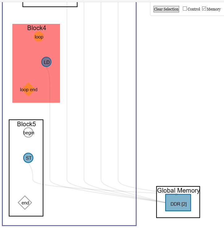
Figure 35. HTML Area Report Showing the Size of the Global Memory Interconnect in an OpenCL Design

In the HTML report, the memory system viewer depicts global memory interconnects as loads (LD), stores (ST), and connections (gray lines).
Figure 36. System Viewer Result of Global Memory Interconnects in an OpenCL Design
The Intel® FPGA SDK for OpenCL Offline Compiler selects the appropriate type of LSU for your OpenCL system based on the memory access pattern of your design. Example LSU types include contiguous access (or consecutive access) and burst-interleaved access. Contiguous Memory Accesses and Optimize Global Memory Accesses illustrate the difference in access patterns between contiguous and burst-interleaved memory accesses, respectively.