Visible to Intel only — GUID: sam1395329942388
Ixiasoft
1. Intel FPGA Integer Arithmetic IP Cores
2. LPM_COUNTER (Counter) IP Core
3. LPM_DIVIDE (Divider) Intel FPGA IP Core
4. LPM_MULT (Multiplier) IP Core
5. LPM_ADD_SUB (Adder/Subtractor)
6. LPM_COMPARE (Comparator)
7. ALTECC (Error Correction Code: Encoder/Decoder) IP Core
8. Intel FPGA Multiply Adder IP Core
9. ALTMEMMULT (Memory-based Constant Coefficient Multiplier) IP Core
10. ALTMULT_ACCUM (Multiply-Accumulate) IP Core
11. ALTMULT_ADD (Multiply-Adder) IP Core
12. ALTMULT_COMPLEX (Complex Multiplier) IP Core
13. ALTSQRT (Integer Square Root) IP Core
14. PARALLEL_ADD (Parallel Adder) IP Core
15. Integer Arithmetic IP Cores User Guide Document Archives
16. Document Revision History for Intel FPGA Integer Arithmetic IP Cores User Guide
7.1. ALTECC Encoder Features
7.2. Verilog HDL Prototype (ALTECC_ENCODER)
7.3. Verilog HDL Prototype (ALTECC_DECODER)
7.4. VHDL Component Declaration (ALTECC_ENCODER)
7.5. VHDL Component Declaration (ALTECC_DECODER)
7.6. VHDL LIBRARY_USE Declaration
7.7. Encoder Ports
7.8. Decoder Ports
7.9. Encoder Parameters
7.10. Decoder Parameters
Visible to Intel only — GUID: sam1395329942388
Ixiasoft
8.1.2. Systolic Delay Register
In a systolic architecture, the input data is fed into a cascade of registers acting as a data buffer. Each register delivers an input sample to a multiplier where it is multiplied by the respective coefficient. The chain adder stores the gradually combined results from the multiplier and the previously registered result from the chainin[] input port to form the final result. Each multiply-add element must be delayed by a single cycle so that the results synchronize appropriately when added together. Each successive delay is used to address both the coefficient memory and the data buffer of their respective multiply-add elements. For example, a single delay for the second multiply add element, two delays for the third multiply-add element, and so on.
Figure 15. Systolic Registers
x(t) represents the results from a continuous stream of input samples and y(t) represents the summation of a set of input samples, and in time, multiplied by their respective coefficients. Both the input and output results flow from left to right. The c(0) to c(N-1) denotes the coefficients. The systolic delay registers are denoted by S-1, whereas the –1 represents a single clock delay. Systolic delay registers are added at the inputs and outputs for pipelining in a way that ensures the results from the multiplier operand and the accumulated sums stay in synch. This processing element is replicated to form a circuit that computes the filtering function. This function is expressed in the following equation.
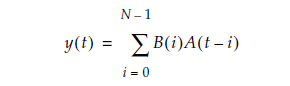
N represents the number of cycles of data that has entered into the accumulator, y(t) represents the output at time t, A(t) represents the input at time t, and B(i) are the coefficients. The t and i in the equation correspond to a particular instant in time, so to compute the output sample y(t) at time t, a group of input samples at N different points in time, or A(n), A(n-1), A(n-2), … A(n-N+1) is required. The group of N input samples are multiplied by N coefficients and summed together to form the final result y.
The systolic register architecture is available only for sum-of-2 and sum-of-4 modes. For both systolic register architecture modes, the first chainin signal needs to be tied to 0.
The following figure shows the systolic delay register implementation of 2 multipliers.
Figure 16. Systolic Delay Register Implementation of 2 Multipliers
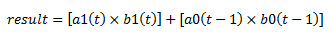
The sum of two multipliers is expressed in the following equation.
The following figure shows the systolic delay register implementation of 4 multipliers.
Figure 17. Systolic Delay Register Implementation of 4 Multipliers
The sum of four multipliers is expressed in the following equation.
Figure 18. Sum of 4 Multipliers

The following lists the advantages of systolic register implementation:
- Reduces DSP resource usage
- Enables efficient mapping in the DSP block using the chain adder structure