Visible to Intel only — GUID: jba1434040229634
Ixiasoft
1.6.1. Initial Stackup Entry
1.6.2. Using the Correct Number of Power/Ground Via Pairs
1.6.3. Using the Correct Number of Power/Ground Via Pairs and Layer Number
1.6.4. Corrected Number of Power/Ground Via Pairs and Layer Numbers
1.6.5. Moving Supplies to Optimal Layers
1.6.6. Moving Power and Ground Planes Closer Together
1.6.7. Move Decoupling Capacitors to the Top Surface of the PCB
1.6.8. Using X2Y Decoupling Capacitors
1.6.9. Using Ultra–Low ESR Bulk Capacitors
1.6.10. Swapping VCC on Layer 9 with VCC, VCCT_GXB, and VCCR_GXB on Layer 4
1.6.11. Assessing How Much Total Capacitance Might be Required
1.6.12. Using the Core Clock Frequency and Current Ramp Up Period Parameters
1.6.13. Overall Design Study Capacitor Savings
1.6.14. Overall Summary
1.6.15. References
Visible to Intel only — GUID: jba1434040229634
Ixiasoft
1.6.6. Moving Power and Ground Planes Closer Together
The impedance plots imply the challenge is in meeting the target impedance at high frequencies. Higher frequency decoupling can be achieved by increasing the capacitance of the power and ground supply planes. This can be achieved by moving the power and ground plane pair closer to each other.
Increasing the surface area of the power and ground plane pair also increases the inter-plane capacitance. The default PDN Tool plane size is used throughout this application note. You can change the plane capacitance and resistance for each power group in the PDN Tool.
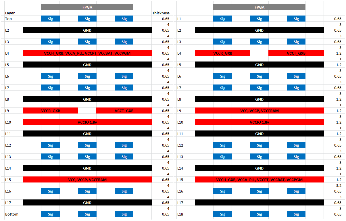
Reducing the original stackup power and ground separation to 1 mil from 4 mils should show an improvement. In the following example, in order to reduce plane resistance, the plane thickness of the power/ground pairs has been increased to 1.2 mil. The figure below compares the original layer-stack (left) with the new stack (right).
Figure 17. Original Stackup (Left) Versus Revised Stackup with Thinner Power and Ground Plane Separation (Right)
The PDN Tool shows that moving the power and ground planes closer together increases the VCC supply Feffective to 36.71MHz.
Figure 18. VCC Supply Feffective after reducing the Power and Ground Plane Separation

Moving the power and ground planes closer together reduces the number of decoupling capacitors for the VCCR_GXB supply to 239. More than 301 capacitors are still required for VCC and VCCT_GXB.
Figure 19. Capacitors Required for the VCC, VCCT_GXB, and VCCR_GXB Supplies after Reducing the Power and Ground Plane Separation
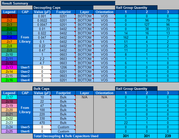
Figure 20. VCC, VCCT_GXB, and VCCR_GXB Supply PDN Performance after Reducing the Power and Ground Plane Separation
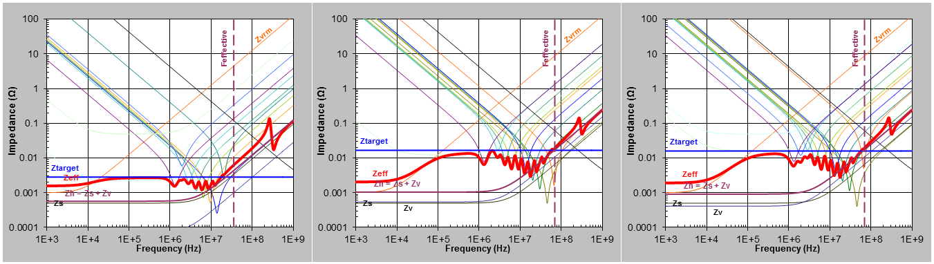
It is clear that improvements in the PCB result in better VCC performance and requires fewer PCB decoupling capacitors for the VCCR_GXB supply but optimization is still required.